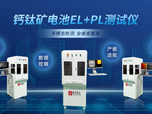
YHG‑ELPL 贯穿研发到量产的全链路检测方案
During the critical transition of perovskite PV from lab to fab, defect inspection capability directly determines efficiency ceiling, stability level and production yield. Yohasolar Laser’s YHG‑ELPL Perovskite EL+PL Tester has been widely deployed in academic research, industrial R&D, pilot validation and production QC, delivering a replicable, quantifiable and traceable standardized inspection solution for customers.
A PV lab at a top‑tier university used the YHG‑ELPL for synchronized EL+PL imaging on samples with varying annealing temperatures and compositions during perovskite interface engineering and stability studies. PL clearly shows grain boundaries, pinholes and composition segregation; EL directly reveals current paths, contact defects and series inhomogeneity. Combined dual‑mode data helped the team build a correlation model of “defect type – process parameter – degradation mechanism”, leading to publications in top international journals and significantly shortening the cycle from basic research to application.
A leading domestic PV enterprise’s perovskite R&D center adopted the YHG‑ELPL during single‑junction and tandem cell development. For key parameters such as precursor concentration, spin‑coating speed, annealing profile and transport layer thickness, it quickly completed multi‑batch comparative tests: PL monitored film uniformity and defect density; EL evaluated current distribution and contact reliability. The device shortened the R&D cycle by 30% and boosted lab yield from 70% to 85%, providing a stable, reproducible process window for pilot scaling.
A perovskite pilot base deployed the YHG‑ELPL on its 300×300mm large‑size cell pilot line as the core validation equipment for process stability and scale‑up feasibility. With a cycle time ≤1 second and resolution ≥0.1mm/pixel, it enabled fast full‑batch imaging and defect grading. By continuously tracking EL/PL pattern changes, the team rapidly identified and corrected process drifts in deposition, annealing and encapsulation, stabilizing pilot yield above 82% and successfully bridging lab to mass production.
Multiple domestic flexible and silicon‑perovskite tandem mass production lines deploy the YHG‑ELPL at final inspection stations, enabling 100% inline inspection, automatic grading and barcode‑based traceability for cells. EL rejects hidden cracks, dark spots and poor contact; PL strictly controls hidden defects such as grain boundaries, pinholes and composition inhomogeneity. The system automatically generates defect reports and thermal maps, quickly locating abnormal processes and driving continuous improvement. Mass production yield stabilizes above 90%, with defect rate reduced by 60%, significantly lowering rework and after‑sales costs while improving product consistency and market reputation.
University Research Case: Visualizing Micro Defects, Accelerating Mechanism Research & Publications
A PV lab at a top‑tier university used the YHG‑ELPL for synchronized EL+PL imaging on samples with varying annealing temperatures and compositions during perovskite interface engineering and stability studies. PL clearly shows grain boundaries, pinholes and composition segregation; EL directly reveals current paths, contact defects and series inhomogeneity. Combined dual‑mode data helped the team build a correlation model of “defect type – process parameter – degradation mechanism”, leading to publications in top international journals and significantly shortening the cycle from basic research to application.
Industrial R&D Case: Formula Screening + Process Iteration, Yield Improvement of 15%+
A leading domestic PV enterprise’s perovskite R&D center adopted the YHG‑ELPL during single‑junction and tandem cell development. For key parameters such as precursor concentration, spin‑coating speed, annealing profile and transport layer thickness, it quickly completed multi‑batch comparative tests: PL monitored film uniformity and defect density; EL evaluated current distribution and contact reliability. The device shortened the R&D cycle by 30% and boosted lab yield from 70% to 85%, providing a stable, reproducible process window for pilot scaling.
Pilot Line Case: Process Stability Validation, Bridging Lab to Mass Production
A perovskite pilot base deployed the YHG‑ELPL on its 300×300mm large‑size cell pilot line as the core validation equipment for process stability and scale‑up feasibility. With a cycle time ≤1 second and resolution ≥0.1mm/pixel, it enabled fast full‑batch imaging and defect grading. By continuously tracking EL/PL pattern changes, the team rapidly identified and corrected process drifts in deposition, annealing and encapsulation, stabilizing pilot yield above 82% and successfully bridging lab to mass production.
Mass Production Case: 100% Full Inspection + Grading & Traceability, Stable Yield Above 90%
Multiple domestic flexible and silicon‑perovskite tandem mass production lines deploy the YHG‑ELPL at final inspection stations, enabling 100% inline inspection, automatic grading and barcode‑based traceability for cells. EL rejects hidden cracks, dark spots and poor contact; PL strictly controls hidden defects such as grain boundaries, pinholes and composition inhomogeneity. The system automatically generates defect reports and thermal maps, quickly locating abnormal processes and driving continuous improvement. Mass production yield stabilizes above 90%, with defect rate reduced by 60%, significantly lowering rework and after‑sales costs while improving product consistency and market reputation.
Customer Value Summary
- ✅ Research Value: Visualized micro defects, interpretable mechanisms, accelerated publications
- ✅ R&D Value: Fast iteration, comparable data, significant yield improvement, shorter cycles
- ✅ Production Value: Full inspection to prevent outflow, grading for quality, traceability for improvement, cost reduction
- ✅ Long‑term Value: Unified inspection standards, data accumulation, supporting technical iteration and capacity expansion
文章关键词: